 |
This chapter describes the structure of a computer from the point of view Level 1 - the Microprogramming level. First we will give an overview of how a processor and memory function together to execute a single machine instruction. Then, a sequence of machine instructions - a program.
We will then build up a real Central Processing Unit (CPU) from subsystems - ALU, Registers etc. We will consider a CPU to consist of three primary parts:
A fourth part, main memory, is never far from the CPU but from a logical point of view is best kept separate.
We will pay most attention to the data path part of the processor, and what must happen in it to cause useful things to happen - to cause program instructions to be executed.
Finally, we will briefly describe how the control part can be implemented by microprogram, i.e. how the decoding of a machine instruction can lead to the execution of a set of sequencing steps called a microprogram.
Note on terminology: the term `microprogram' came about before microprocessors were ever dreamt of. It refers to a program in which each instruction is concerned with a very small event - like the sending of the contents of a register to the ALU.
Before you continue, you should review the material on multiplexers, decoders, ALUs, registers, buses, etc. in the previous chapter.
Figure 5.1 shows the data path part of our hypothetical CPU from [Tanenbaum, 1990], page 170 onwards.
Here, we briefly describe the components of Figure 5.1. Then we give a qualitative discussion of how it executes program instructions. Finally we describe the execution of instructions in some detail.
There are 16 identical 16-bit registers. But, they are not general purpose, each has a special use:
A and B latches hold stable versions of A and B buses. There would be problems if, for example, AC was connected straight into the A input of the ALU and, meanwhile, the output of the ALU was connected to AC, i.e.. what version of AC to use; the answer would be continuously changing.
As described in Figure 4.2.2 above. Recall that the ALU may perform any of four functions:
Any other functions have to be programmed.
The shifter is not a register - it passes the ALU output straight through: shifted left, shifted right or not shifted.
The MAR is a register which is used as a gateway - a `buffer' - onto the address bus. Likewise the MBR (it might be better to call this memory data register) for the data bus.
The ALU input A can be fed with either:
The memory is considered to be a collection of cells or locations, each of which can be addressed individually, and thus written to or read from. Effectively, memory is like an array in Java or any other high-level language. For brevity, we shall refer to this memory `array' as M and the address of a general cell as x and so, the contents of the cell at address x as M[x], or m[x].
To read from a memory cell, the controller must cause the following to happen:
To write to a memory cell, the controller must cause something similar to happen:
It is a feature of all general purpose computers that executable instructions and data occupy the same memory space. Often, programs are organised so that there are blocks of instructions and blocks of data. But, there is no fundamental reason, except tidiness and efficiency, why instructions and data cannot be mixed up together.
To describe the details of operation of the CPU, we use a simple language called Register Transfer Language (RTL). The notation is as follows. M[x] denotes contents of location x; sometimes m[x], or even just [x]. Think of an envelope with £100 in it, and your address on it.
Reg denotes a register; Reg = PC, IR, AC, R1 or R2.
[M[x]] denotes contents of the address contained in M[x]. Think of an envelope containing another envelope.
We use ![]() to denote transfer:
to denote transfer: ![]() . Pronounce this as `A gets B'.
In the case of
. Pronounce this as `A gets B'.
In the case of ![]() , we say `A gets contents of x'.
, we say `A gets contents of x'.
Note: There is a world of difference between an address, 100, say, and data value contained in that address.
How does the CPU and its controller execute a sequence of instructions?
Let us start by considering the execution the instruction at location 100Hex; what follows is an endless loop of the so-called fetch-execute cycle:
Start off with PC = 100H - PC is the Program Counter, and is used to address the instruction (data) to be fetched and executed.
In previous versions of this course, I used to go into complete detail of the microprogram which controls the CPU - the microprogram implements the Fetch-(Decode)-Execute cycle. This time I'm going to leave it out. If interested, see section 5.9 appended to this chapter, or [Tanenbaum, 1990], section 4.2.2 onwards.
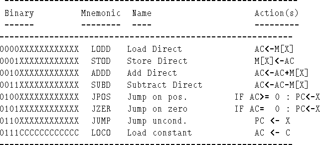
We now examine the instruction set, by which Level 2 programmers can program the machine; if in doubt, we call these macroinstructions.
Incidentally, you could program in microcode - but life is too short, just like life is too short to program in assembly (macro) code, if you can do it in Java, C, or C++.
We will call the level 2 machine Mac-1a; Mac-1a is a restricted version of Tanenbaum's Mac-1). The main characteristics of Mac-1a are: data word length 16-bit; address size 12-bits.
Exercise: What is the maximum number of words we can have in the main memory of Mac-1a? (neglect memory mapped input-output). How many bytes?
There are two addressing modes : immediate and direct; we will neglect Tanenbaum's local and indirect for the meanwhile.
It is accumulator based: everything is done through AC; thus, `Add' is done as follows: put operand 1 in AC, add to memory location, result is put in AC.
The Mac-1a programmer has no access to the PC or other CPU registers. Also, for present purposes, assume that SP does not exist.
A limited version of the Mac-1 instruction set is shown in Figure 5.2.
The columns are as follows:
As stated earlier, there are no direct instructions for input- output; instead Mac-1a uses memory-mapped input-output, whereby some memory cells are mapped to input-output ports; for simplicity we assume that there are only two ports, one connected to a standard-input device, the other connected to a standard-output device:
We assume that each device works with bytes (i.e. 8-bits).
A read from address 0FFCHex yields a 16-bit word, with the actual data byte in the lower order byte. There is no use in reading the input port until the connected device has put the data there: so 0FFDH is used to read the input status register; the top bit (sign) of 0FFDH is set when the input data is available (DAV).
Thus, a read routine should go into a tight loop, continuously reading 0FFDHex, until it goes negative; then 0FFCHex can be read to get the data. Reading 0FFC clears 0FFD again.
Output, to 0FFE, runs along the same lines as input. A write to 0FFE will send the lower order byte to the standard-output device. The sign bit of 0FFFH signifies that the device is in a ready to receive (RDY) state; again there is no use writing data to the output port until the device is ready to read it.
As discussed, control of the CPU - fetch, decode, execute - is done by a microcontoller which obeys a program of microinstructions.
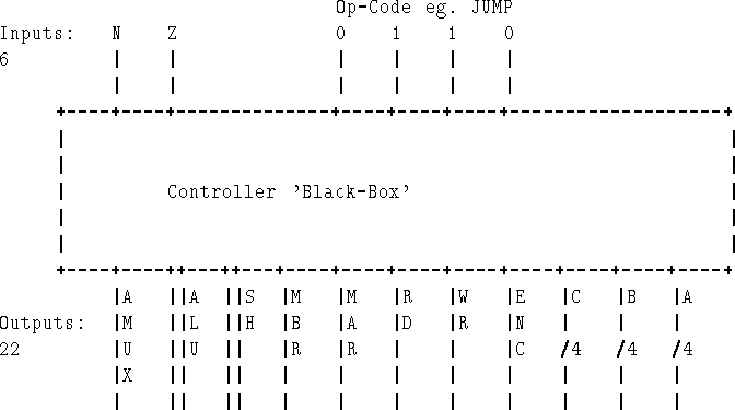
We might think of the microcontroller as a `black-box' such as that shown in Figure 5.3.
You can think of it as a black-box which has a set of inputs and a set of outputs - just like any other circuit, ALU, multiplexer, etc. Therefore, instead of microprogramming, it can be made from logic hardware.
To design the circuit, all you have to do is prepare a truth-table (6 input columns - op-code (4 bits) and N, Z, 22 output columns), and generate the logic.
There is no reason why this hardware circuit could not decode an instruction in ONE clock period, i.e. a lot faster than the microcode solution.
The microprogrammed solution allows arbitrarily complex instructions to be built-up. It may also be more flexible, for example, there were many machines that users could microprogram themselves; and, there were computers which differed only by their microcode, perhaps one optimised for execution of C programs, another for COBOL programs.
On the other hand, if implemented on a chip, control store takes up a lot of chip space. And, as you can see by examining [Tanenbaum, 1990], microcode interpretation may be relatively slow -- and gets slower, the more instructions there are.
Machines with large sets of complex (and perhaps slow) instructions (implemented with microcode), are called CISC - complex instruction set computer.
Those with small sets of relatively simple instructions, probably implemented in logic are called RISC - reduced instruction set computer.
Most early machines - before about 1965 - were RISC. Then the fashion switched to CISC. Now the fashion is switching back to RISC, albeit with some special go-faster features that were not present on early RISC.
CISC machines are easier to program in machine and assembly code (see next chapter), because they have a richer set of instructions. But, nowadays, less and less programmers use assembly code, and compilers are becoming better. It comes down to a tradeoff, complexity of `silicon' (microcode and CISC) or complexity of software (highly efficient optimising compilers and RISC).
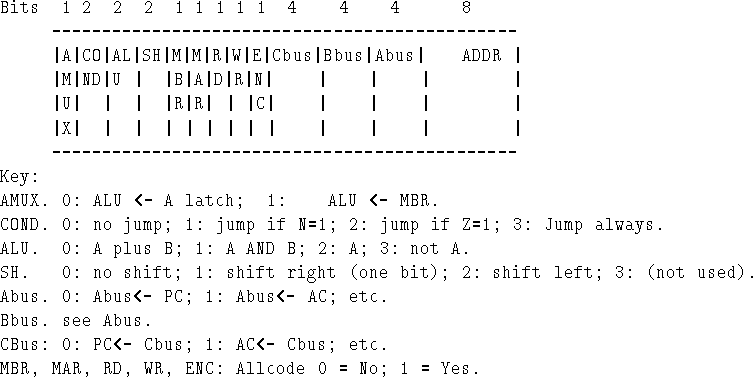
To control the data path in Figure 5.1 we need 61 different signals:
If we have decoded a macro-instruction and know the values of the 61 signals then it is possible to execute the macro-instruction i.e.. perform one cycle of the data path. [From now on instruction = macro-instruction; micro-instruction will never be shortened.]
We could always work with a 61-bit micro-instruction register - whose outputs are connected to the right places. However, many savings are possible:
12 saved.
12 saved.
2 saved.
1 extra.
2 saved.
Thus the size of micro-instruction register = 61 - (12+12+12+2+2-1) = 22 bits.
Figure 5.4 shows microinstruction layout, with two new fields: ADDR and COND, which are used by the microcontroller, to control itself.
Example. Here is the microinstruction which performs the execute part of a
JUMP instruction. ![]() .
.
A four phase clock is used. There are four phases or subcycles:
And that is it - one cycle of the data path operation; but note that it takes more than one of these cycles to execute a macro-instruction.
Figure 5.5 shows the completed microarchitecture.
The components of the microcontrol part are now explained.
Often micro-instructions follow in numerical order, i.e. ![]() does the sequencing.
does the sequencing.
But, as with conventional programs, may need to break normal sequence. I.e. jump . The COND field states conditions under which jump may take place (including never).
If a jump is required, ![]() (via Mmux). The box Micro seq.
logic actually controls Mmux, but for clarity, this connection is not shown
in Figure 5.5.
All this happens at clock phase 4, when ALU flags N, Z are stable.
(via Mmux). The box Micro seq.
logic actually controls Mmux, but for clarity, this connection is not shown
in Figure 5.5.
All this happens at clock phase 4, when ALU flags N, Z are stable.
We assume, as is usual, that it takes more than one micro- instruction cycle to Read or write to memory (assume 2 cycles). Thus if you start a Read in cycle n by asserting RD, you must ensure that RD is asserted in cycle n+1; in fact the whole n+1th microinstruction can be RD alone. But, that would be wasteful, and clever microprogrammers can usually find something useful to fill the time.
Example. We require to add AC to A and store result in AC. This microinstruction would do that:
ENC=1, C=1, B=1, A=10(decimal); fields not mentioned = 0
This is one way of writing it. You could also write out the 32 bits in full (as they would appear in control store or in MIR). However, that would be tedious and error prone. It is better to use a high-level language notation. Thus, we will use RTL, supplemented with:
Figure 5.6 illustrates the resultant MicroAssembler Language or MAL, and how it translates into numeric microinstructions (we use decimal, instead of binary, to save space) .
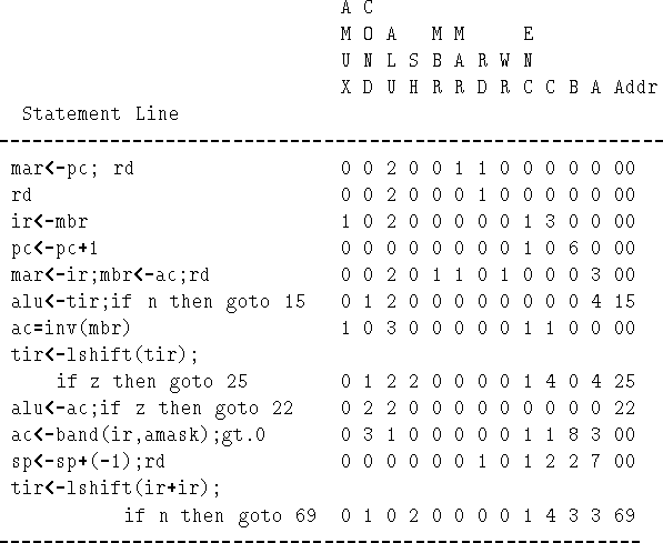
Figure 5.7 show the full microprogram that runs on Mic-1 and interprets (fetches-decodes-executes) Mac-1A instructions.
As described earlier, the microprogram continuously loops on:
Line 0 starts by fetching contents of PC; RD is asserted.
Line 1 just holds RD high (we need 2 cycles for memory access); it increments PC while it is waiting.
Line 2 gets the instruction into IR; it also passes IR through ALU to test bit 15; if bit 15 is set then we jump to 0 ( no instructions in Mac-1a has bit 15 set - check in Figure 5.4-4).
Note the subtraction algorithm (see Chapter 2 for discussion of twos
complement etc.). If x and y are binary:
Exercise.
Simulate, by tracing on paper, the execution of the STOD instruction: STOD is at location 100, it is storing to location 543. Assume PC = 100, AC = 4321.
(a) Write down the contents of all registers at the start.
(b) Ditto for all relevant memory locations, i.e. 100 and 543.
(c) Step through the microcode, from line: 0; note each line visited; write down the contents of any register changed by the microinstruction.
(d) When you get back to line: 0 write down the contents of all registers and all relevant memory locations.
(e) Use (a), (b) and (d) to verify that STOD did what it was meant to do.
Answer.
(a) Write down the contents of all registers at the start.

PC = 100, AC = 4321, others don't care.

(b) Ditto for all relevant memory locations, ie. 100 and
543.

[100] = 1543; [543] = don't care.

(c) Step through the microcode, from line: 0; note each line
visited; write down the contents of any register changed by
the microinstruction.

0: mar<-pc;rd;

     mar = 100; RD set;

1: pc<-pc+1;rd;

     pc = 101; RD set;

2: ir<-mbr;if n then goto 0;

     mbr = 1543; ir = 1543; n=FALSE (0);
     1543 = 0001 0101 0100 0011

3: tir<-lshift(ir+ir); if n then goto 19;

     alu output = 0010 1010 1000 0110
     shf output = 0101 0101 0000 1100
     tir      = 0101 0101 0000 1100
     n = FALSE (0)

4: tir<-lshift(tir); if n then goto 11;

     alu output = 0101 0101 0000 1100 (NB NOT shifted yet)
     shf output = 1010 1010 0001 1000
     tir      = 1010 1010 0001 1000
     n = FALSE (0) (because bit 15 of alu is 0)

5: alu<-tir; if n then goto 9;
     alu output = 1010 1010 0001 1000
     Finally, n = TRUE (1),
     so, we go to 9.

9: mar<-ir;mbr<-ac;wr;

     mar = 0101 0100 0011 (543 - it only holds 12 bits)
     mbr = 4321;
     WR set.

10:wr; goto 0;
     WR set
     [543] = 4321 at the end of this microcycle.

(d) When you get back to line: 0 write down the contents of all registers
    and all relevant memory locations.

     pc = 101, ac = 4321, [543] = 4321,
     remainder don't care.

(e) Use (a), (b) and (d) to verify that STOD did what it was meant
to do.

I think so!
a0 = a1 +
  a2
:
   lodd a1
   addd a2
   stod a0
Taking into account the fetch-execute cycle, and that there is a controller
which also uses MAR and MBR, and assuming that the program starts at 100Hex
(lodd a1 is there), and that a0, a1, a2 are at
100Hex, 101Hex, and 102Hex, respectively, describe precisely, and in order,
all the data travel along the bus, to and from memory. Distinguish addresses
and data.
a<-a+a; if n then goto 0;
a<-lshift(a); if n then goto 0;
1100 1000 0001 0001 1001 0000 0000 1000
1111000000000000 as its machine code.
0111000000000000 as its binary code. What is significant about
that code. Analyse your implementation to see if it is any faster than the
'old' Mac-1A method.