This chapter describes the intermediate sized building blocks of computers, i.e. those which are intermediate between simple gates at one extreme, and full microprocessors on a chip at the other extreme. With an understanding of these components we will be able to describe the construction of a working computer - next chapter.
Most of the circuits below are available as CMOS or TTL MSI packages.
In a microprocessor such as a Pentium III, obviously these packages are not used; however, if you examined the circuit diagram for a microprocessor, you would find similar `building blocks' used throughout the chip.
Before you proceed, make sure that you have attempted exercises 17-20 of chapter 3.
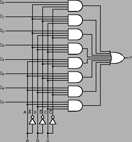
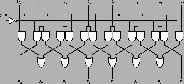
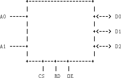
A multiplexer (mux) connects via switches a number (typically, some power of
two, 2n) of input lines to one output line; see
Figure 4.1
shows and eight input multiplexer. A, B, C are the
selection (or switching or control or address) lines; when ![]() , input D0 - and no
other input - is fed through to F.
, input D0 - and no
other input - is fed through to F.
A demultiplexer does the opposite to a multiplexer: it has one input, and many 2n) outputs. A demultiplexer uses select/address lines just as the multiplexer, i.e. the appropriate output is addressed by the select lines.
Exercise. Construct a truth-table for the eight-input multiplexer shown in Figure 4.1 and thereby verify that it does as promised, i.e. F =D0 when (A, B, C) = (0, 0, 0), etc.
Exercise. By examining Figure 4.1,
derive an expression for Fin terms of ![]() . Check it for
. Check it for ![]() .
.
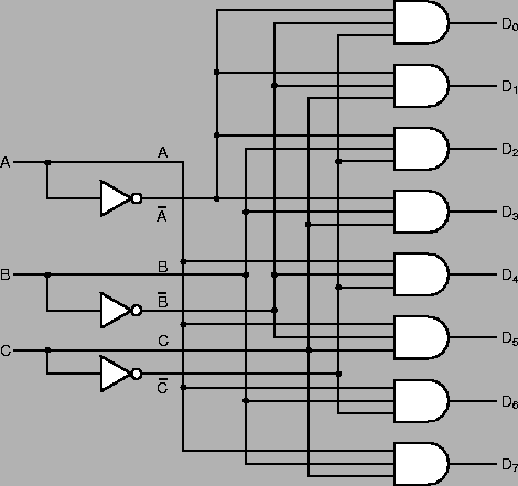
A decoder takes n inputs, has 2n outputs, and, according to the select/address lines, one (and one only) of the outputs goes to a logic 1.
In principle, a decoder operates like a demultiplexer, but with a logic 1 tied to the (single) input all the time, i.e. in a decoder, the selected output goes to 1. Figure 4.2 shows a 3-to-8 decoder.
Exercise. By examining Figure 4.2,
derive an expression for Fin terms of ![]() . Check it for
. Check it for ![]() .
.
Consider the following application of a decoder: a hotel with 8 (23) rooms needs to send room identity, e.g. for fire-alarm, to a central location. Instead of using eight lines, being knowledgeable of computer science, they decide to use just three lines, and code the room identity as a three bit number. But, they want any alarm to light one of eight lights; hence, they need a 3-to-8 decoder.
Similarly, in a computer, it may be wasteful to use eight lines for eight actions: so code them and transmit them as three bits, then decode for use.
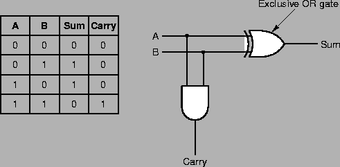
A half adder, shown in Figure 4.3
together with its truth-table adds together two single bit inputs bits to give a
sum bit S, and a carry bit C. We see that ![]() ; and C = A.B.
; and C = A.B.
Exercise. Think back to our mention of (decimal) addition using carries, e.g. 6804 + 1236 (6 + 4 is 10, put down 0 and carry one ... Considering that, discuss whether the half-adder makes sense.
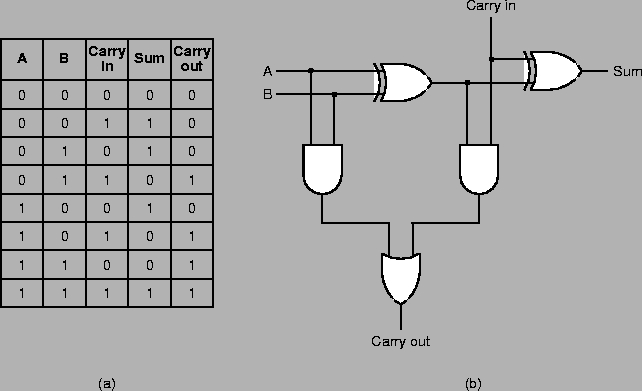
The full-adder is a bit more useful; the inputs are two bits to be added, plus carry - from another previous addition. A full-adder may be built from half-adders and an OR gate, see Figure 4.4.
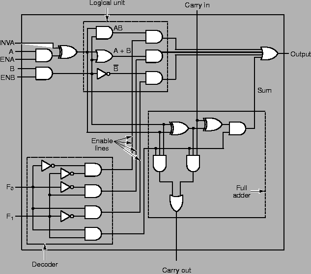
Getting more ambitious, Figure 4.5
shows a one bit ALU. It uses two function bits F0,
F1 - bottom left-hand corner - to choose between four possible
operations: ![]() In addition, via
INVA,
In addition, via
INVA, ![]() may be substituted for A in any of
the four. Moreover, either A or B, or both, may be enabled via
may be substituted for A in any of
the four. Moreover, either A or B, or both, may be enabled via
![]() ; if ENx is 1then the value for
x is enabled (allowed to pass into) the circuit, otherwise 0 is
passed in.
; if ENx is 1then the value for
x is enabled (allowed to pass into) the circuit, otherwise 0 is
passed in.
Notice the full adder on the bottom right, and the decoder, see section 4.1.2, on the bottom left.
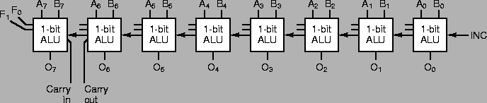
We can make an n-bit ALU by connecting n one bit ALUs together; such an 8 bit ALU is shown in Figure 4.6. In some contexts, such one bit circuits (or sometimes more than one) are called `bit-slices'.
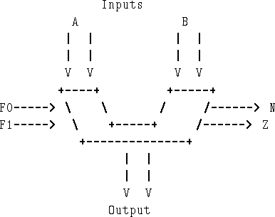
In the next chapter we will use an ALU, viewed functionally as a subsystem, like that in Figure 4.7.
It can computer four functions and these are selected by (input)
control lines ![]() . The functions are:
. The functions are: ![]() .
.
Two condition flags are output, which give the `condition' of the result of the last operation. These are: N, set to 1 if the last operation caused a negative result, Z, set to 1 if the last operation resulted in zero.
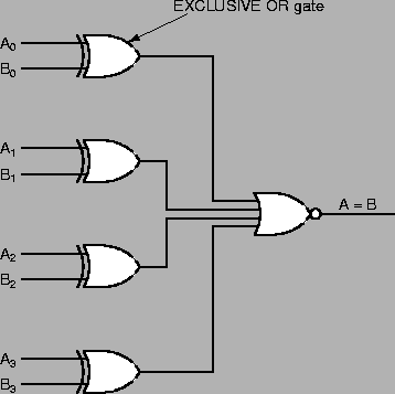
Figure 4.8 shows a four bit magnitude comparator.
Figure 4.9 shows an eight bit shifter. C=1 shifts right, C=0 shifts left.
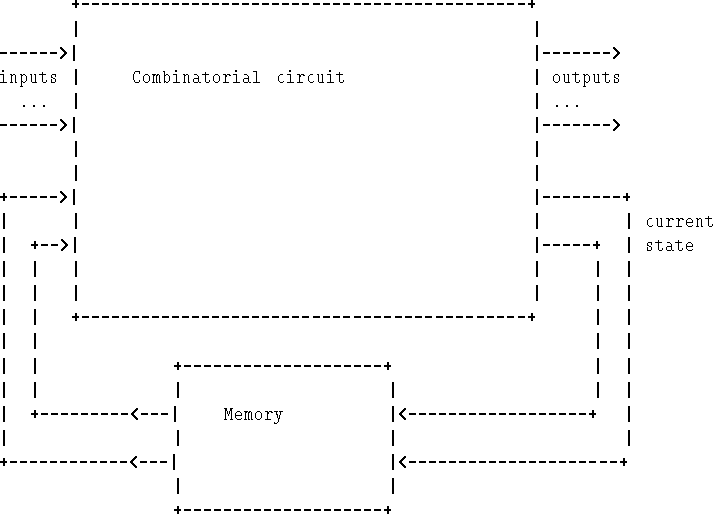
Up to now, we have dealt with combinatorial logic, i.e. the outputs depend only on the current inputs - the outputs disappear when the inputs disappear. In many cases, definitely in a computer, we require retention of state - memory. Digital circuits with memory are called sequential circuits.
After showing a theoretical model of sequential circuits, we will describe some basic memory circuits - flip-flops, etc. Then section 4.4 will give an overview of larger memory subsystems such as are used as the main memory of computers.
A sequential circuit can be modelled as a separate combinatorial circuit connected to memory or storage, as shown in Figure 4.10. However, this diagram is useful only from a theoretical point of view, and, in practice, the memory and gates are all mixed up.
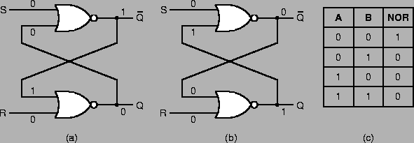
[Incidentally, the terms `latch' and `flip-flop' tend to get mixed up; [Tanenbaum, 1999] makes the distinction that latches are level triggered, whilst flip-flops are edge triggered, see section 4.3 below.
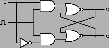
Figure 4.11 shows a Set-Reset(SR) latch implemented with nor gates.
Two inputs: S, R; one Sets - output goes to 1, the other Resets
- output goes to 0. Two outputs: ![]() ,
which are inverses of one another.
,
which are inverses of one another.
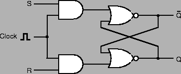
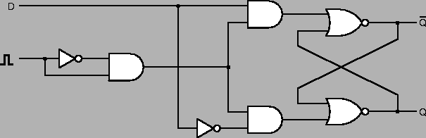
It is often important to restrict changes to specified times which are
specified by a clock pulse - also called enable or strobe.
See Figure 4.12.
In this case, ![]() get through the and gates only
when the clock pulse is present (1).
get through the and gates only
when the clock pulse is present (1).
Figure 4.13 shows a D-type latch; this gets rid of the nonsense of S = R = 1 together, i.e there is only one input, D (Data).
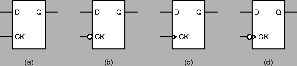
Enabling/clocking with a level is uncomfortable for engineers. Edges or transitions are better - they are more clearly defined. Thus, D-type edge triggered, see Figure 4.14 for a circuit.
Figure 4.15 shows the symbols used for some D-type latches and flip-flops. CK stands for clock, a circle on it signifies clocked by 0level, or falling edge - as opposed to level 1, or rising edge.
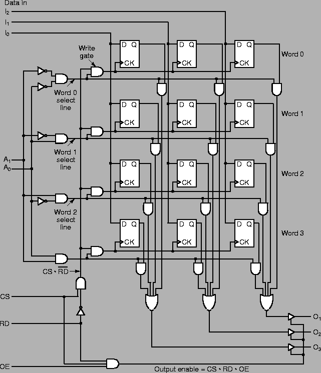
It would be possible to make a (main) memory, or individual registers, from D-type flip-flops, but pretty impractical if you need a number of Megabytes. And, it's not only that multi-million chips is a problem, but the multi-million lines in and out, not to mention the clock lines.
Figure 4.16 shows the logic diagram for a four word three-bits memory system.
It is instructive to understand how it works in principle, because all bigger chips operate similarly.
This is reflected in the schematic diagram (summary) shown in Figure 4.17.
With little more added, the decoding and enabling schemes shown in Figure 4.16 can be used to handle input-output ports as well as memory. Thus, some memory addresses are retained, e.g. FFF0Hex to FFFF Hex, and when, e.g. a memory write is performed to FFF0Hex, this does not go to memory, but to an output port, which in turn is connected to some output device. Likewise, memory-mapped input.
On PC compatibles, the screen graphics is represented by data in memory. This memory resides in the same memory space as ordinary memory. Hence, writing to appropriate (low) memory addresses can change the text or graphics on the screen.
Conceptually, a register is no different from a main memory word.
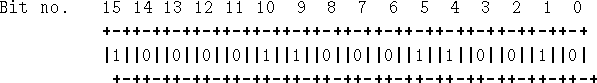
A 16-bit Register can store 16 bits, see Figure 4.18. Please note the numbering scheme for bits (now fairly universally agreed).
When we talk of CPU registers, we usually mean registers located in the CPU; these may be special purpose - and so not directly addressable by programmers -, or general purpose, in which case they are addressed by some alphanumeric code (e.g. AC, or X, or R1). Because of the speed of the memory making up the register, and/or its proximity, data transfer to and from a CPU register is normally an order of magnitude faster than main memory access.
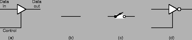
Don't worry, you don't have to learn a new calculus of a logic with three logic states! Simply, as well as 1 and 0, a tri-state buffer can have a third state: disconnected or open-circuit, i.e. it operates purely as an electronic switch. A control line operates the switch. See Figure 4.19.
 |
Crudely, a bus is a pipeline along which data can flow; but, usually, it's not as simple as connecting two devices with wires, usually the bus is multi-purpose and can be used by a number of devices; the devices must take their turn; thus, in addition to the physical connection, we need to define rules - these rules are called the bus protocol.
In general, you can have many devices connected by the same bus. Like a group of people talking - or even closer analogy, a group of people on a telephone conference - some order has to be preserved. Not everyone can talk at once. A bus has no problem with many listeners - but there can only be one talker at any one time - a bit like a lecture!)
Essentially, bus = physical connection + protocol.
In its simplest form a bus is controlled by a master, who handles requests, from slaves to use the bus.
The complexity of the protocol depends on how general purpose is the design of the bus. Internal computer buses can be simple; external buses, which may be used for printers, analogue interfacing etc., need a well specified protocol.
For the meanwhile, think of a bus as a pipe along which data flow, and access to the bus is controlled by a system of `taps'; the taps are often in the form of multiplexers on the input to the bus, and tri-state buffers on the output.
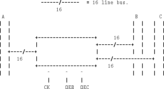
Figure 4.20 shows a 16-bit register connected to buses C, A and B.
The signals OEB, OEC open tri-state buffers to allow, respectively, the contents of the register onto bus B, or bus C, or both; the controller which handles OEB, OEC ensures that this register will never be enabled onto any bus (B, or C) at the same time any other register is enable onto that bus - let us reiterate: a bus can tolerate no more than one talker.
Whilst one must use tri-state to output-enable each register that is connected to a bus, normally, a multiplexer is sufficient to select between multiple buses capable of writing to a register. In addition, a clock (CK) operates to select when the data actually gets clocked into the register.
Note the shorthand for a multi-line bus.
ROM = Read-only-memory. RAM = Random-access-memory.
But, unfortunately, the names are misleading. Both are in fact Random Access, or Direct Access - as opposed to Sequential Access. ROM is so-called because, usually, it is only ever written to once, and thereafter is only read (i.e. Read Only).
Random access means that you can access any memory sell on demand; you can read the addresses in any order;
Sequential access means that to get to memory address N, you
have to read address ![]() , finally, N;
, finally, N;
Sequential access is more common in disk and tape files; in that case, a record contains, not only its own data, but a pointer to the next record. In a random access disk file, there is a table, at the beginning of the file, giving the pointers to all records.
The circuit discussed in section 4.4
is a four word ![]() -bit RAM; you can read and write, and both
read and write are random access.
-bit RAM; you can read and write, and both
read and write are random access.
A ROM is logically quite similar, except you cannot write it in the normal way; it is fixed during manufacture; or it written with special equipment - PROM, Programmable ROM. ROM stays the same even when the power is off: it is non-volatile. Thus: RAM: Read/Write, volatile; ROM: Read only, non-volatile
Nearly everything in a computer happens on the rising (or falling - depends on convention) edge of a pulsed signal (the computer's equivalent of a `beat' or orchestra conductor's hand signals. Thus, we need a clock, which produces a periodic sequence of pulses. The period - or cycle time - is typically around 0.01 microsecond, 0.01 x 10⁻⁶ secs which is 0.01 of a millionth of a second.
A period of 0.01 microsecs implies a clock rate (or frequency
of 100MHz. 100 MegaHertz is ![]() cycles per second.
cycles per second.
In what follows times (t and T) are measured in seconds, and frequencies, f, in Hertz (Hz); Hertz is a synonym for cycles per second; Hertz is credited with the discovery of radio-waves. The period - usually denoted T - of a periodic event (a repetitive event) is the time between the beginning of one event and the beginning of the next one; e.g. if the event 0 starts at t = 0.0, event 1 at t = 0.1, event 2 at t = 0.2, etc. the period T = 0.1 seconds.
The frequency (or rate) refers to the number of events that happen in one second; thus the events above have a frequency of 10 cycles per second, or 10 Hz.
It is a simple matter to convert from period (T) to frequency (f):

We need shorthand for large frequencies, and small times; it is common practice to deal in multiples of 103:
Note the difference between m - milli-, 10-3, and M - Mega, 106 !
Exercise. If the period is 0.002 ![]() sec, or
sec, or ![]() , what
is the clock rate? Ans:
, what
is the clock rate? Ans: ![]() .
.
Exercise. If you wanted a clock rate of 1000 MHz what is the period? Ans: 1 nsec.
Q. If you had a 750 MHz PC, i.e. one on which the clock `beats' at a rate of 750 million beats per second, could it do 750 million adds per sec.? A. Definitely no. There are two main reasons:
(a) Verify this statement using a truth table.
(b) Draw a diagram for a two-input multiplexer - see Figure 4.1.
(c) A four input multiplexer will have four inputs - and one output; how many control lines (A, B, C, ...); again, see Figure 4.1.
(d) Sketch a diagram for a four-input multiplexer.
(b) Hence, or otherwise, draw a block diagram for a two-bit full adder.
(c) Hence, or otherwise, draw a block diagram for an n-bit full adder - who only the lower two components, and the top one.
(a) Convince yourself that the decoder subsystem (bottom left-hand corner) does its work properly; name the output lines, respectively from the top, Fand, For, FcompB, Fsum, and determine what values of (F0, F1) generate these signals.
Note the use of and gates to enable the appropriate outputs into the output or gate.
(b) ENA, ENB are used to enable (or the opposite -
block) A and B into the logic and adder units; likewise
INVA is used to cause A to be replaced by ![]() ,
explain qualitatively, how, using both F0,
F1 and ENA,
ENB, INVA, you would generate:
,
explain qualitatively, how, using both F0,
F1 and ENA,
ENB, INVA, you would generate: ![]() , A `straight-through', B
`straight-through',
, A `straight-through', B
`straight-through', ![]() `straight-through'.
`straight-through'.
(b) Draw a similar diagram for ![]() memory.
memory.
(b) How many memory locations can be addressed using 12 address lines.