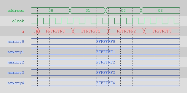
The following waveforms show the behavior of altsyncram megafunction for the chosen set of parameters in design mem.v. For the purpose of this simulation, the contents of the memory at the start of the sample waveforms is assumed to be ( FFFFFFF0, FFFFFFF1, FFFFFFF2, FFFFFFF3, ...). The design mem.v has one read/write port. The read/write port has 256 words of 32 bits each. The core uses a different clock enable than the input registers. The output of the read/write port is unregistered.
The above waveform shows the behavior of the design under normal read conditions. The read happens at the rising edge of the enabled clock cycle. The output from the RAM is undefined until after the first rising edge of the read clock. The clock enable on the read side input registers are disabled.
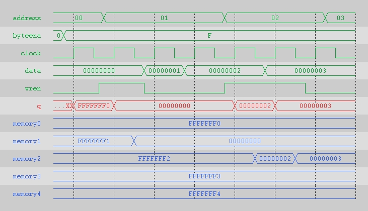
The above waveform shows the behavior of the design under normal write conditions. The write cycle is assumed to be from the rising edge of the enabled clock in which wren is high till the rising edge of the next clock cycle. Actual write into the RAM happens at the falling edge of the write clock. The clock enable on the write side input registers are disabled. During a write cycle, the new data flows through to the output.
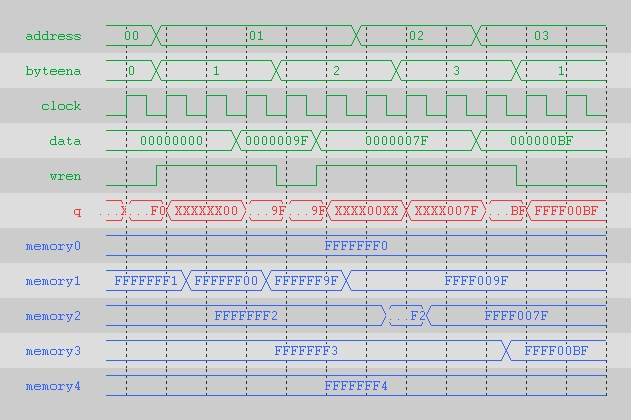
The above waveform shows the behavior of the design under write conditions using byteenable ports. During the write cycle, only the bytes that are being written to flow through and the disabled bytes show up as unknown in the output in the write cycle.