VLSI = Very Large Scale Integration
| Nomenclature | Active Device Count | Typical Functions |
|---|---|---|
| SSI | 1-100 | gates, op-amps, many linear applications |
| MSI | 100-1000 | registers, filters, etc. |
| LSI | 103-104 | microprocessors, A/D converters, etc. |
| VLSI | > 104 | memories, computers, signal processors |
The steady down-scaling of CMOS device dimensions has been the main stimulus to the growth of microelectronics and the computer industry over the past two decades. The more an IC is scaled, the higher becomes its packing density, the higher its circuit speed, and the lower its power dissipation. Today, after many generations of scaling, the smallest feature in a CMOS transistor is approaching atomic dimensions and off-state leakage current per transistor has been rising because thermal energy does not scale. So how much longer can CMOS scaling continue?
As the integration level of ICs moves toward 100 million transistors in the next few years, key issues of transistor design must be reexamined for 0.100.13-µm generation technology. In previous CMOS generations, it was possible to disregard many parasitic components like off-state leakage and gate current. But in the not-so-distant future, these undesirables will grow rapidly as the fundamental limits imposed by thermodynamics and quantum mechanics close in on the technology.
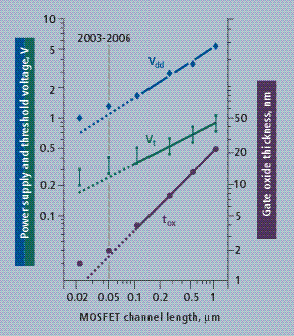
As IC manufacturing techniques progress, CMOS devices with shorter channel lengths will switch faster and use less power. Lower power-supply and threshold voltages (Vdd and Vt) and thinner gate oxides (tox) will accompany the shrinking channel lengths. Transistors built between the years 2003 and 2006 will have a minimum channel length of 0.05 µm, a power supply voltage of 1.2 V, and a threshold voltage near 0.25 V.
Reference: Yuan Taur, The Incredible Shrinking Transistor, Spectrum, July, 1999 25-29.
|
VENDOR |
FEATURE
SIZE |
PROCESS |
NOTES |
| AMI | 0.50µ | C5N | 3 metal, 2 poly, high res, non-silicided, 5V |
| AMI | 1.20µ | ABN | 2-metal, 2-poly, NPN, 5V |
| HP | 0.25µ | CMOS07 | 5-metal, 1 poly, silicided, 1.8V |
| HP | 0.35µ | GMOS10QA | 4-metal, 1-poly, silicided, 3.3V |
| HP | 0.50µ | AMOS14TB | 3-metal, 1-poly, linear cap, silicide block, 3.3V |
| Supertex | 2.00µ | SCNA20 | 2-metal, 2-poly, NPN, 5V |
| Peregrine | 0.50µ | SOI-SOS 0.5µ | 3 metal layers, various options, SOS |
| TSMC | 0.25µ | TSMC 0.25µ | 5-metal, 1-poly, silicided, 2.5/3.3V |
| TSMC | 0.35µ | TSMC 0.35µ |
3-metal, 2-poly, polycided, 3.3/5V *OR* 4-metal, 1-poly, silcided, 3.3/5V |
See MOSIS web site for more information.
| Minimum feature size of process technology | 0.1 mm |
| Total number of transistors | 200 million |
| Number of logic transistors | 40 million |
| Number of logic transistors | 40 million |
| Chip size | 520 mm2 |
| Clock frequency | 2.0-3.5 GHz |
| Number of I/O connections | 4000 |
| Number wiring levels | 7-8 |
| Supply voltage | 0.9-1.2 v |
| Supply current | about 160 A |
| Power dissipation | 160 W A |
Table 1 Technology Generations
|
Year of First Product Shipment |
1997 |
1999 |
2002 |
2005 |
2008 |
2011 |
2014 |
|
Technology NodeDense Lines (DRAM Half-Pitch) (nm) |
250 |
180 |
130 |
100 |
70 |
50 |
35 |
|
Isolated Lines (MPU Gates) (nm) |
200 |
140 |
100 |
70 |
50 |
35 |
25 |
|
Memory |
|||||||
|
Generation @ samples/introduction (bits) |
256M |
1G |
4G |
16G |
64G |
256G |
1T |
|
Generation @ production ramp (bits) |
64M |
256M |
1G |
4G |
16G |
64G |
256G |
|
Bits/cm 2 @ sample/introduction |
96M |
270M |
770M |
2.2B |
6.1B |
17B |
48B |
|
Logic (high-volume, cost-performance: MPU) † |
|||||||
|
Logic transistors/cm 2 (packed, including on-chip SRAM) |
3.7M |
6.2M |
18M |
39M |
84M |
180M |
390M |
|
Logic (low-volume: ASIC)** ‡ |
|||||||
|
Usable transistors/cm 2 (auto layout) |
8M |
14M |
24M |
40M |
64M |
100M |
160M |
** ASIC—application-specific integrated circuit
1998 Updates are in Red.
Table 2 Chip Size
|
Year of First Product Shipment |
1997 |
1999 |
2002 |
2005 |
2008 |
2011 |
2014 |
|
Technology NodeDense Lines (DRAM Half-Pitch) (nm) |
250 |
180 |
130 |
100 |
70 |
50 |
35 |
|
Isolated Lines (MPU Gates) (nm) |
200 |
140 |
100 |
70 |
50 |
35 |
25 |
|
Functions/Chip |
|||||||
|
DRAM bits/chip—Years 1–6 |
267M |
1.07G |
4.29G |
17.2G |
68.7G |
275G |
1.10T |
|
Microprocessor total transistors/chip—Years 1–6 |
11M |
21M |
76M |
200M |
520M |
1.40B |
3.62B |
|
Chip size (mm 2) (@sample/introduction) |
|||||||
|
DRAM—Year 1 |
280 |
400 |
560 |
790 |
1120 |
1580 |
2240 |
|
DRAM—Year 3 (2 nd shrink) |
170 |
240 |
340 |
480 |
670 |
950 |
1340 |
|
DRAM—Year 6 (2 nd cut-down-next gen.) |
100 |
140 |
200 |
280 |
390 |
550 |
780 |
|
MPU—Year 1 |
300 |
340 |
430 |
520 |
620 |
750 |
901 |
|
MPU—Year 3 (2 nd shrink) |
180 |
205 |
260 |
310 |
370 |
450 |
540 |
|
MPU—Year 6 (2 nd cut-down-next gen.) |
110 |
125 |
150 |
180 |
220 |
260 |
312 |
|
ASIC (Max litho field area) |
480 |
800 |
900 |
1000 |
1100 |
1300 |
1482 |
|
Lithographic field size area (mm2) |
22 ´ 22 484 |
25 ´ 32 800 |
25 ´ 36 900 |
25 ´ 40 1000 |
25 ´ 44 1100 |
25 ´ 52 1300 |
25 x 59 |
|
Maximum Substrate Diameter (mm) |
|||||||
|
Bulk or epitaxial or SOI** Wafer |
200 |
300 |
300 |
300 |
300 |
450 |
450 |
** SOI—silicon on insulator
1998 Updates are in Red.
Source: International Technology Roadmap
Beginning in 1993 a small group of people at Intel began thinking seriously about a transition from 200mm manufacturing to the next wafer size. By early 1994, the industry reached consensus that the right size was 300mm.
Today, selection teams are in place for all equipment, from materials handling to clean parts, many of them selecting tools for new semiconductor processes never implemented at Intel. The teams are synchronized to produce a first set of tools in January 2000 and high volume 0.13 mm manufacturing capability in the second half of 2002. The productivity, as measured by reduction in die cost, is expected to exceed our targets of 30%. For comparison, only about a 15% productivity increase was achieved in moving from a 150mm to a 200mm wafer size.
Reference: Daniel Seligson, Planning for the 300mm Transition
Maintained by John Loomis, last updated 24 Aug 1999