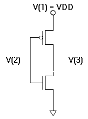
CMOS LOGIC INVERTER

*Enter the voltage sources into SPICE.  The value of VIN can be arbitrary
*because it will be incremented over a range of values by the .DC command

VDD 1 0 5V
VIN 2 0 0V


*Enter the MOSFETs and set the geometrical factors W and L:
*  D G S B
M1 3 2 1 1 PCHAN W=0.75U L=0.5U
M2 3 2 0 0 NCHAN W=0.75U L=0.5U

*Specify the parameters of the two MOSFETs:
.MODEL PCHAN PMOS (VTO=-0.8 KP=21e-6 LAMBDA=0.03)
.MODEL NCHAN NMOS (VTO=0.7 KP=73e-6  LAMBDA=0.01)


*Instruct SPICE to plot the voltage transfer characteristic for 0 < VIN < 5V
.DC VIN 0 5V 0.001V

.PRINT DC V(3)

*Instruct the .PROBE utility to save VOUT during the .DC sweep
.PROBE V(3)

.END