Microelectronics Assignment 9
Do the following exercises for this assignment. Document your work in a
Microsoft Word document or PDF. You must submit your SPICE
schematics and other associated files.
- Layout (in LTSpice) a full-adder. You should have an adder
schematic, an adder symbol, and a simulation schematic that
instantiates the adder. Simulate the operation of
the adder to demonstrate its proper operation.
- Combine your adder and the DFF from assignment 8 to form a
1-bit adder with accumulator. You should create a symbol for this
combination. Report the total number of transistors for your design.
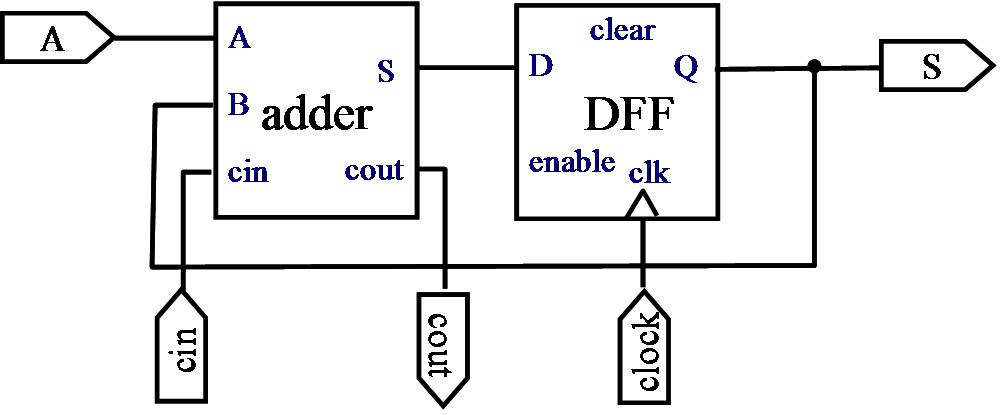
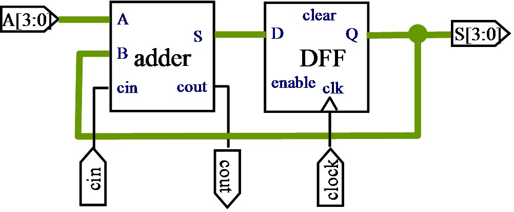
- Combine your adder/accumulator to form a four-bit system.
Create a symbol for this system and a simulation schematic that
replicates the functionality of the system shown below.
Determine the maximum propagation delay.
- Create Verilog and LTSpice versions for your assigned
xorgate.
See xorgates.xlsx for the design assignments.
Verify in both that the gate behaves properly.
- Create circuit and layout cells for your assigned design.
See designs.xlsx for the design assignments.
Duplicate the layout shown as closely as possible. Demonstrate the
functionality of your design. Note: Undergraduates are excused from this problem.
Maintained by John Loomis,
last updated 10 April 2014