Microelectronics Assignment 6
Document your work in a Microsoft Word document or PDF.
Show netlists for all Spice calculations.
You must submit your JELIB files and SPICE
schematics and other associated files.
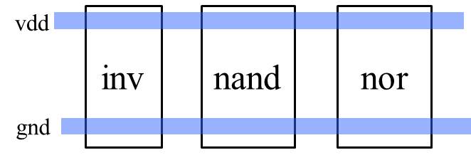
- Revise or design the Electric layout of your inverter and nand gate
in this assignment so that the power rails are at the same relative location
and the gates may be arranged side-by-side as shown below. Document with
the picture of a layout in Electric. The nor gate will be designed later.
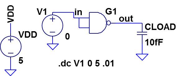
- Revise your nand gate design from the tutorial 4, if necessary, so that the
rise and fall times of the equivalent inverter (inputs connected) are the same.
Show the resulting transfer curve and determine the switch point.
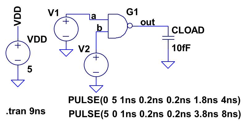
- Create an Electric layout of your device and determine the parastics.
Transfer the parastic parameters to LTSpice, then
measure the rise and fall times of the device as suggested below.
- Measure the dimensions of the source and drains in your nand gate and
determine how Electric calculated the parasitics.
- Construct a colored-paper model of your nand gate or inverter. You may work in
groups to insure that feature sizes are the same.
- Work through tutorial 5 (see link below). Your report should
include layout figures, schematic figures, and other analysis and
diagrams discussed in the tutorial.
Tutorial
5 – Design, layout, and simulation of a ring oscillator – electric_tutorial_5_video.wmv
(22:41)
Maintained by John
Loomis, last updated 10 March 2015