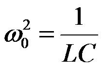
Adjust your choice of components so that the frequency is between 5 kHz and 30 kHz.
| Component | Measured | Calculated |
|---|---|---|
| L | n/a | |
| C | n/a | |
| fo | n/a |
In each of the following exercises you will need to record the following measurements from the oscilloscope.
- Frequency
- Peak-to-peak (amplitude) voltage of the input waveform
- Peak-to-peak (amplitude) voltage of the output waveform
- Phase difference between input and output
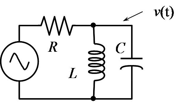
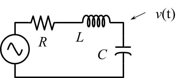
This is a resonant circuit. Adjust the frequency to give maximum output signal. Record the AC response (voltage and phase). Change the frequency higher and lower until the gain (ratio of output to input amplitude) has dropped to 0.707 of the peak gain. The phase shift at this point should be ±45°. Repeat the measurement using a different resistance. Start with a resistance of about 1 kΩ and then about 20 kΩ.
Case 1 (R = )
| Frequency | Vin | Vout | Ratio (gain) | Phase |
|---|---|---|---|---|
Case 2 (R = )
| Frequency | Vin | Vout | Ratio (gain) | Phase |
|---|---|---|---|---|
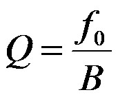
| Case | Measured | Calculated | ||||
|---|---|---|---|---|---|---|
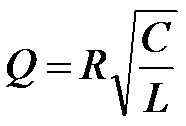
| Resonant frequency | Bandwidth | Q | Resonant frequency | Bandwidth | Q | |
| 1 | ||||||
| 2 | ||||||
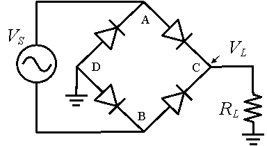
Measure source voltage on oscilloscope with probes between A and B. Measure load voltage with probes between C and D. Do not attempt to measure both signals on the oscilloscope at the same time, the oscilloscope channels share a common ground and trying to make simultaneous measurements will introduce ground loop problems.
Set the frequency of the source to 50 Hz and the amplitude to 10 volts peak-to-peak. Attach oscilloscope images of the source voltage and the load voltage to the report, showing the frequency, maximum voltage, and minimum voltage in each signal. Take several pictures with the input varying from 10 volts to 1 volt peak-to-peak. Determine the input amplitude at which the output signal vanishes.
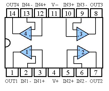
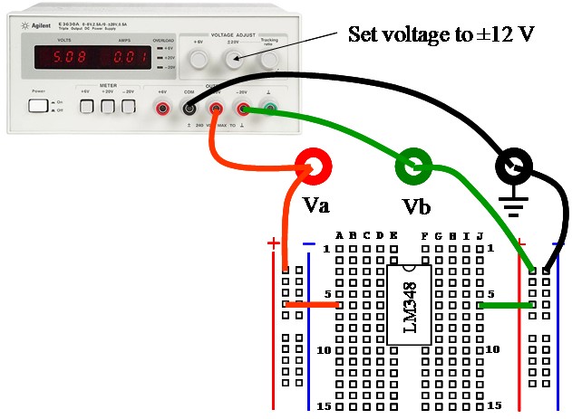
Pin Diagram of LM348 IC
Construct the inverting amplifier circuit shown below, with resistances Rf = 470 kΩ, Rs = 47 kΩ, and RC = 10 kΩ. Calculate the ideal gain and phase shift from the nominal resistance values.
- Measure the gain and phase shift at the following
frequencies.
Frequency 400 Hz 700 Hz 1 kHz 5 kHz 10 kHz 50 kHz - Find the frequency and gain at which the phase has shifted by 20° and shifted by 45°
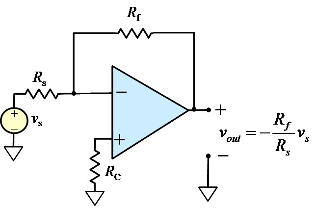
Inverting amplifier