|
| 
|


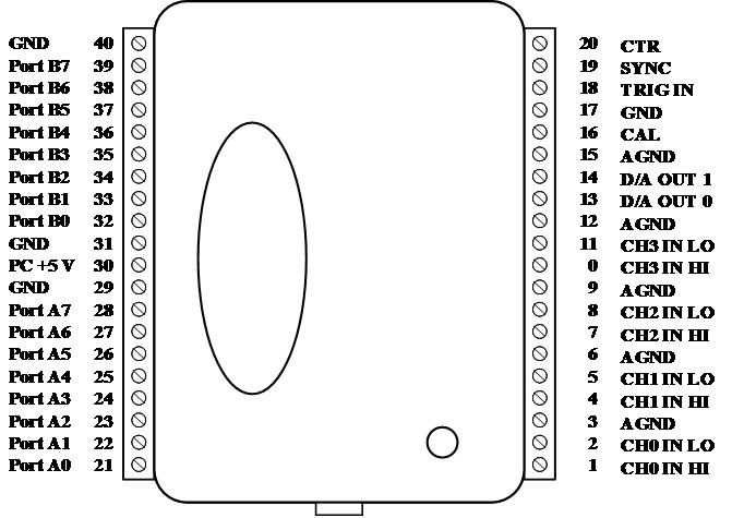
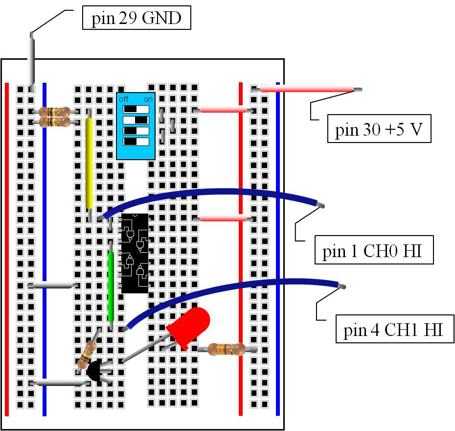
The diagram below suggests how the components might be arranged on a prototype board. The data acquisition system provides power to the circuit. Connect pin 5 (CH1 LO) to pin 6 (AGND).
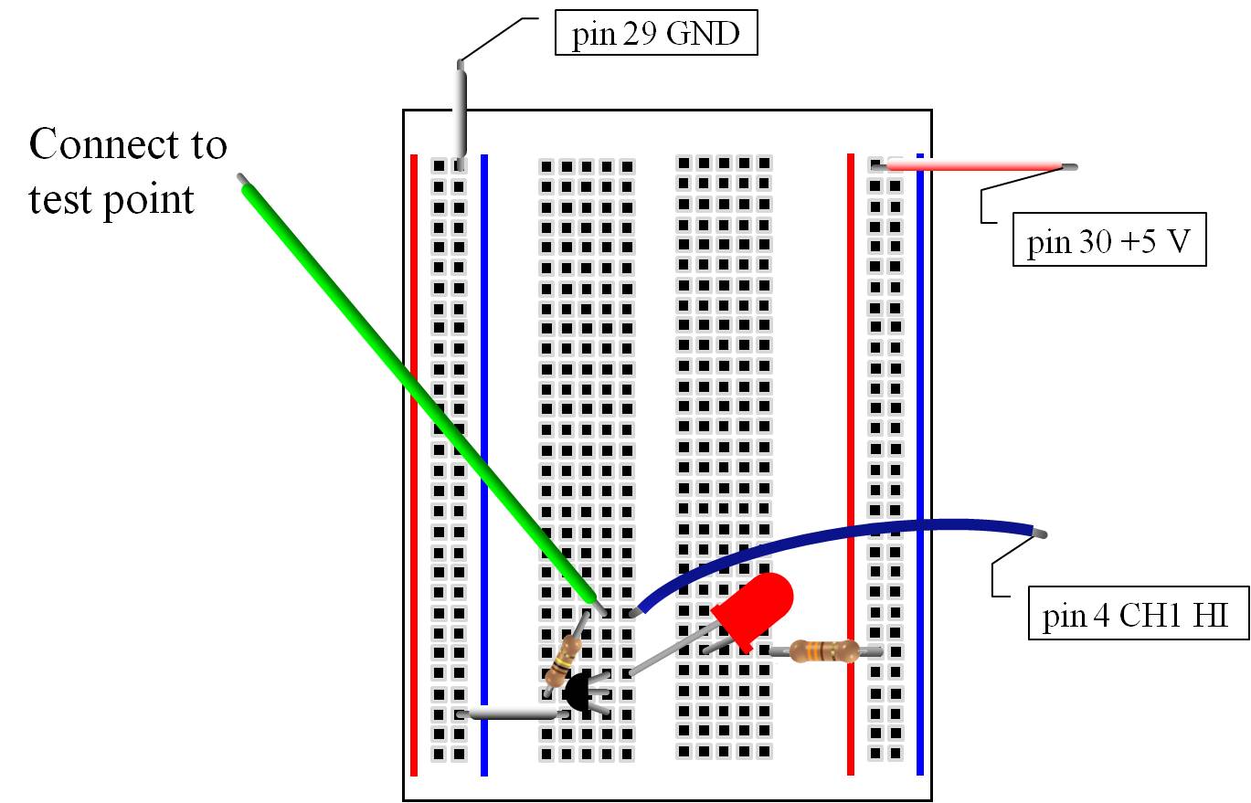
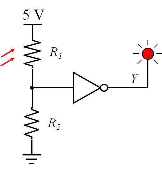
Construct the logic indicator and test it by connecting the input to 5 V and to ground. Measure the voltage across each resistor when the indicator is on, and use Ohm's Law to determine the corresponding currents.
| 
|
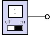
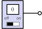
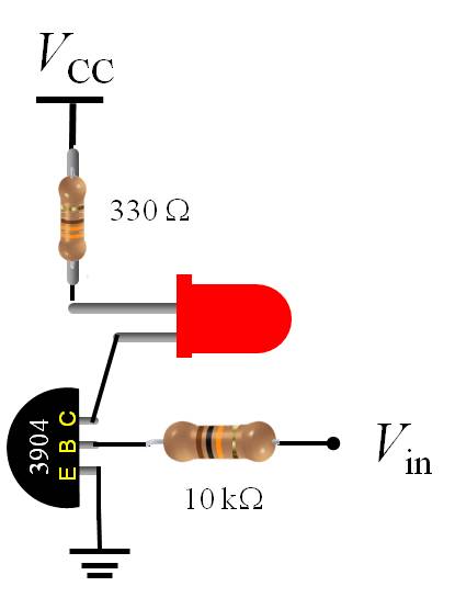
Connect logic switches and logic indicator as shown below. You will eventually need three switches, only two are shown here, and only the top switch is used in this exercise.
Connect the circuit to the DAQ. Turn the top switch on and off and confirm that the LED turns on and off. Collect strip chart data showing the switching behavior.
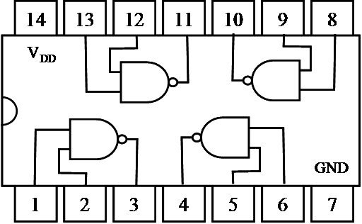
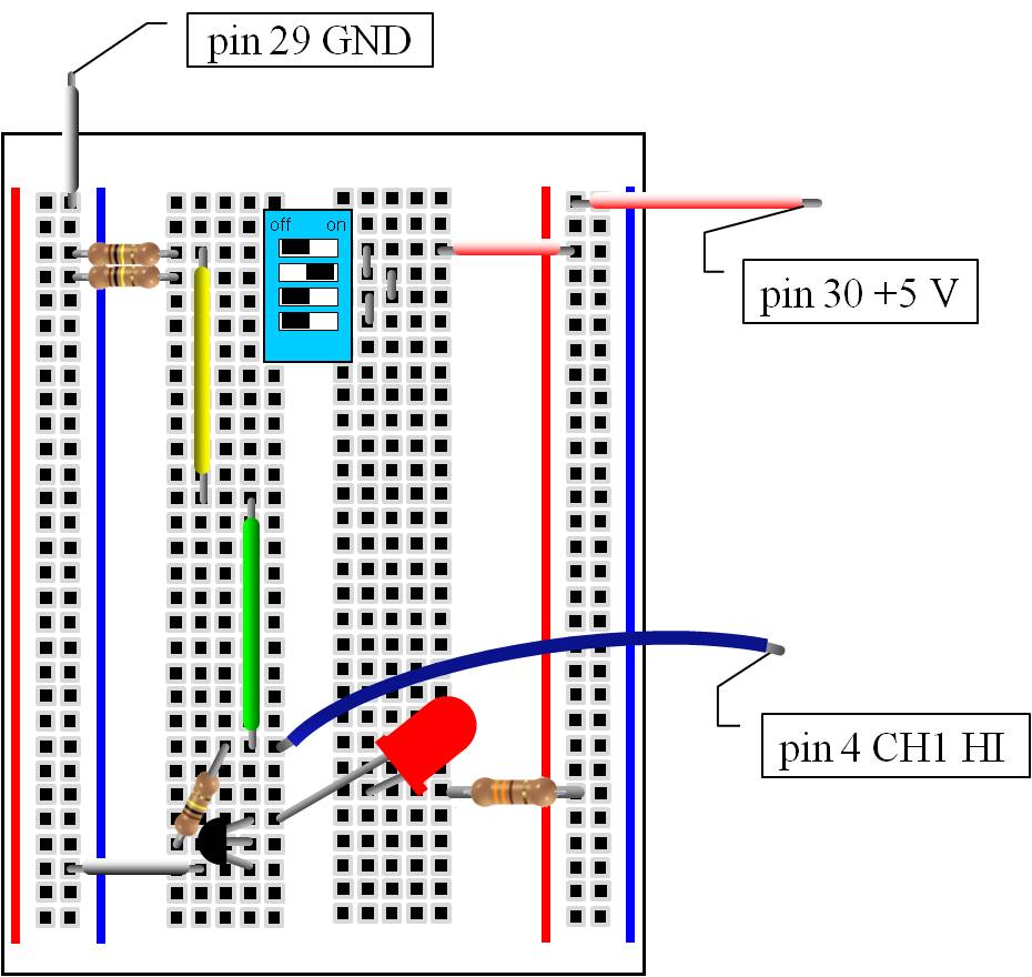
Remember to connect power (5 V - DAQ pin30 - to chip pin 14) and ground (GND - DAQ pin29 - to chip pin 7). Connect DAQ pin 2 (CH0 LO) to DAQ pin 3 (AGND).

Connect Vin to the top switch and to pin 1 (CH0 HI) of the DAQ. Connect the output Vout to pin 4 (CH1 HI). Connect pin 5 (CH1 LO) to pin 6 (AGND).
The diagram below shows how the breadboard might look, but is not the only way of arranging the components.
Use the strip chart to display channels 0 and 1 as you manually toggle the switch. Observe and describe the pattern of the indicator light. Include a plot (or screen shot) of the strip chart.
![]()
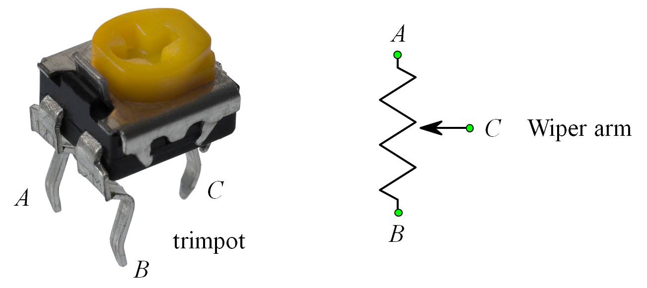
The potentiometer, or trimpot, is shown below.
Collect strip chart data as you vary the potentiometer over its range of motion. Plot the output voltage from the strip chart as a function of the input voltage of the strip chart. This is the transfer curve of the inverter. Identify, as best you can, the voltage at which the inverter switches and the LED turns on or off.